Semiconductor Wafer Fabrication Process
Comments Off on Semiconductor Wafer Fabrication ProcessSemiconductors are vital components in everyday life, powering cars, mobile phones, computers, TVs, and even credit cards. Semiconductor manufacturing is complex, requiring many steps and precisely controlled processes. This blog will shed light on wafer fabrication, the first step of semiconductor manufacturing.
What Is a Semiconductor Wafer?
Semiconductors serve as substrates for building microelectronic devices that control the flow of electric current. A semiconductor wafer is a thin slice of semiconductor material used in electronics for manufacturing microchips, integrated circuits (ICs), photovoltaics, solar cells, and other semiconductor devices. Substrate wafers are essential components of modern electronic devices like computer chips, smartphones, and cameras.
Semiconductor wafers are typically made from very pure single-crystal silicon or other semiconductor materials like:
- Germanium
- Silicon germanium (SiGe)
- Gallium arsenide (GaAs)
- Sapphire (Al2O3)
- Indium phosphide (InP)
- Silicon carbide (SiC)
- Zinc oxide (ZnO)
- Gallium nitride (GaN)
- Diamond
Semiconductor wafer diameters range from 25.4 mm to 450 mm, and thickness varies based on mechanical strength and material properties. Wafers smaller than 200 mm in diameter typically have flats to indicate crystallographic planes, and wafers 200 mm or larger use a small notch for orientation.
Semiconductor Wafer Fabrication Process
Making a semiconductor wafer is a complex process that requires operators to follow strict standards with high precision. The following steps describe the process of semiconductor wafer fabrication.
- Creating an Ingot: After silicon is extracted from sand, it is purified using a heating and refining process. The purified silicon is then melted into a high-purity liquid and solidified through crystallization to form a silicon ingot. Only ultra-high purity ingots are fit for semiconductor use.
- Slicing the Ingots into Thin Wafers: Operators use sharp diamond saw blades to slice the ingots into thin wafer discs. The diameter of the ingot determines the wafer’s size. Thinner wafers lower manufacturing costs, and larger wafers increase the number of semiconductor chips produced per wafer. As a result, wafers are trending thinner and larger.
- Grinding: Surface grinding corrects issues like waviness from wire sawing. The grinding process produces high-quality wafers and can sometimes replace rough polishing and lapping.
- Rounding: A diamond disk smooths the edges of sawn wafers to remove damage and ensure the wafer is the required diameter.
- Lapping: Wafers then go through lapping, a mechanical process using pads and slurry to flatten and polish. This step removes excess silicon and surface damage to give the wafer a dull grey, semi-reflective finish.
- Polishing: Polishing gives the wafers a mirror-like finish and helps prevent breakage and warping. The process also makes them thinner and more flexible.
- Cleaning: Various cleaning methods—including pre-diffusion, RCA, mega sonic, and ozone cleaning—are used to remove contamination from the wafer due to air exposure.
- Patterning: The cleaned wafer is then patterned in a process called photolithography. A light-sensitive layer, or photoresist, is applied to the wafer, followed by a mask on top of the wafer. This mask contains a pattern that corresponds to the required electronic component to be produced. The wafer is then exposed to UV light, which transfers the pattern from the mask to the photoresist.
- Doping: Through ion implantation, certain impurities are added to the wafer to change its electrical properties. Boron and phosphorus are commonly used to create p-type and n-type semiconductors.
- Deposition: Thin films of material are deposited onto the wafer to create the desired electronic components. Various techniques for deposition include physical vapor deposition, chemical vapor deposition, and atomic layer deposition.
- Etching: Plasma etching, wet etching, or dry etching removes specific parts of the wafer, shaping it according to the intended electronic component.
- Inspection: By comparing photos of different dies, specialized tools inspect the wafers for defects. The most common technologies used for inspection include electron-beam inspection and brightfield inspection.
Need Coils for Semiconductor Wafer Fabrication?
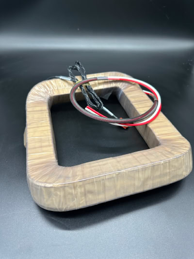
The semiconductor wafer fabrication process depends on highly precise, controlled RF and electromagnetic coils. During deposition, doping, and etching, magnetic coils generate the necessary electromagnetic fields of different sizes, strengths, and consistencies to give the semiconductor wafers different properties.
Custom Coils specializes in designing, engineering, and manufacturing coils for semiconductor manufacturing, such as electromagnets for dielectric and polysilicon etching. Contact us to get started on your semiconductor wafer fabrication project today.


